2 Layer PCB Board

2 Layer PCB Board

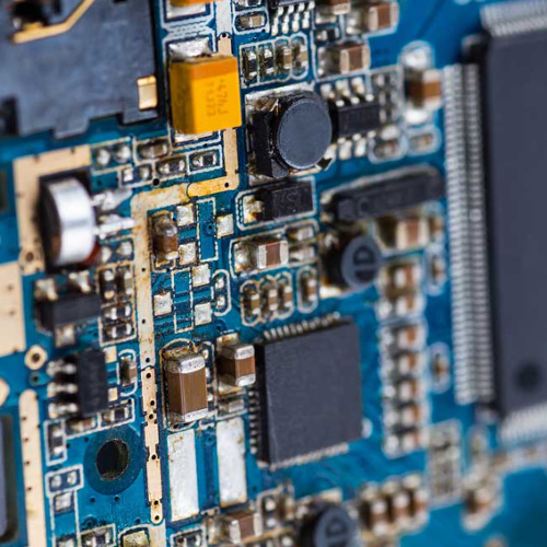
2 Layer PCBs are the most common type of PCB. Plus, 2 layer PCBs are also known as double-sided PCBs because they have components on both sides of the board.

The 2-layer pcb fabrication is by bonding two layers of copper together with a dielectric material in between. And the dielectric material can be either an FR-42 or an FR-44.

Furthermore, the copper on each side can carry different electrical signals, which makes them ideal for applications where high speed and/or dense packaging is necessary. 2 Layer PCBs are also the most economical type of PCB to manufacture.

Using a PCB ground plane provides advantages in terms of signal integrity, power integrity, routing, and noise:

EMI/EMC

Placing a ground plane below signals reduces their inductive susceptibility to EMI. In other words, it helps suppress crosstalk from inside the board and noise induced from sources outside the board. Placing a ground plane on the bottom layer of a two-layer PCB provides noise reduction; it reduces the loop area seen by signals.

Stable switching

The grounded path followed by signals will have lower inductance, which helps create a lower inductance ground connection that reduces ground bounce. It will also be easier to place and route any caps needed for stable power.

Solvability

It’s easy to route back to ground in a 2-layer board with a ground plane; just drop a via and connect it directly to ground. You’ll save a lot of space that would otherwise be used to route ground traces or rails. In 2-layer boards, including dense boards that won’t have the EMI/EMC and SI/PI problems I mentioned, using a 2 layer PCB ground plane is also preferable to just routing ground traces. Nearly every board that includes multiple components will simply not have enough room for routing return traces alongside all signal traces. Placing a PCB ground plane below the relevant components and signal traces also allows you to route ground returns directly from a component to the ground plane through a via. The return signal will then follow the path of least impedance back to the power supply return. This also allows you to easily place bypass/decoupling capacitors between power connections on critical components and the PCB ground plane, which allows any high frequency fluctuations in the power connection (e.g., conducted EMI from a switched power supply) from reaching the relevant components.