- +61-416631973
- alcomgrouppty@gmail.com
- NSW , Australia
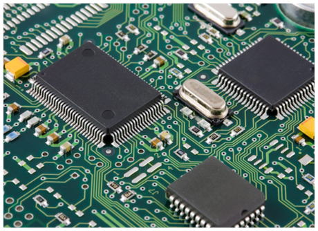
Printed circuit board (PCB) design has grown into its own specialized field within the electronics industry. PCBs play an important role in that they provide electrical interconnections between electronic components, rigid support to hold components, and a compact package that can be integrated into an end product. They are the main component in an electronic device that is responsible for form and function, and they allow advanced semiconductors to communicate with each other at very high data rates.
All PCBs are built from alternating layers of conductive copper with layers of electrically insulating material. Conductive features on printed circuit boards include copper traces, pads, and conductive planes. The mechanical structure is made up of the insulating material laminated between the layers of conductors. The overall structure is plated and covered with a non-conductive solder mask, and silk screen is printed on top of the solder mask to provide a legend for electronic components. After these fabrication steps are completed, the bare board is sent into printed circuit board assembly, where components are soldered to the board and the PCBA can be tested.
Alcom Group company vision to reach in every sector of industries which wants to give best service with value of price. The dream of the company who join the hands everyone has to develop with their skills and ability to make success.
©2019. Alcom Group. All Rights Reserved.
WhatsApp us