- +61-416631973
- alcomgrouppty@gmail.com
- NSW , Australia
PCB stands for printed circuit board and it’s the foundation of many electronics. It provides electrical connections between components on the circuit, including resistors and capacitors.
These connections can be made with a single layer of copper, but when you build more complex circuits, you need to add more layers of copper to accommodate additional connections. When you build a double-layer PCB, you’re stacking two layers of copper together in order to create more complex circuitry.
Hence, a double-layer PCB is one that has two copper layers. This is a common technique used in making circuit boards, and it can be used to help reduce the number of connections through the board, as well as increase its flexibility.
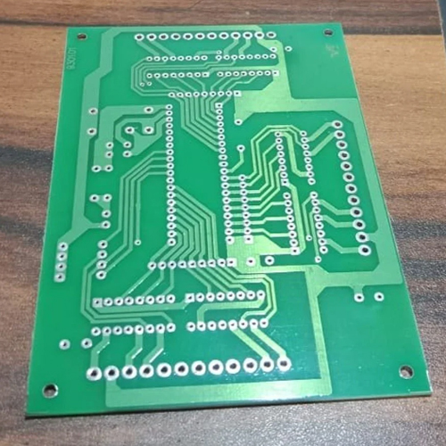
A Double Layer PCB or a double-sided PCB is a thin layer of directing material, similar to copper, connected to both the best and base sides of the board. It is extremely useful in many electronic applications because circuits on one side of the board can be connected on the other side of the board with the help of holes drilled on the board.
Advantages of double-layer PCB
Alcom Group company vision to reach in every sector of industries which wants to give best service with value of price. The dream of the company who join the hands everyone has to develop with their skills and ability to make success.
©2019. Alcom Group. All Rights Reserved.
WhatsApp us